


Sensing radiation of charged particles X- and γ-rays from radioactive isotopes or nuclear reactions plays a key role in the applications of industrial and medical imaging, as well as homeland security [1-3]. As nuclear detection capabilities are essential to countering chemical, biological, radiological, and nuclear (CBRN) threats, the Department of Defense and the Department of Homeland Security (DHS) have invested in fundamental and applied research to conduct CBRN defense. For example, the Defense Threat Reduction Agency (DTRA) has spearheaded research and development (R&D) efforts in recent years to develop a smaller and more sensitive internal point-detection sensor to alert military ground vehicles to nuclear and radiological hazards [4].
In most cases, nuclear detection requires high sensitivity as well as energy resolving capabilities to obtain fingerprint information of distant, shielded, or weak radiative sources. Currently, scintillators and semiconductors are the two primary means of radiation detection. Large volume scintillators may offer desirable detection efficiency, but poor energy resolution can negatively affect the accuracy of isotope identification. Among scintillation materials, SrI2 :Eu and LaBr3 :Ce demonstrate the most impressive energy resolving capability—2–3 percent for 662 keV γ-ray [5, 6]. This may be worse than CdZnTe (CZT) semiconductor detector (<0.5 percent for 662 keV y-ray) [7], but it is available in large volumes. For most scintillation materials, high energy resolution usually does not parallel with high stopping power or environmental robustness.
Compound semiconductors have been heavily studied since the 1940s [8], and appear to be the best choice for enabling the operation of compact and high performance devices at room temperature (RT). However, few legacy materials are candidates for commercialization—namely, CdTe/CZT, TlBr, and HgI2—in part because production issues impede their use at scale. Among them, CZT has been considered the most promising.
One positive feature of semiconductor detectors (when compared to other types) lies in their ability to capture the real-time, three-dimensional spatial position of radiological chemicals, which has been demonstrated using single pixelated CZT detector unit [1, 9, 10]. Uni-polarity charge-sensing technology is specialized for this functionality by virtue of the fact that the mean free drift length of electrons is larger than hole length by around one order of magnitude in CZT crystal.
The flourishing of CZT began in the 1990s in the U.S. through developing new instruments for astronomy applications at NASA [11]. R&D investment in CZT remains strong, and CZT detector performance and crystal uniformity has gradually improved over the last decade [11]. However, in practice, sophisticated growth furnace and experiences from trial-and-error experiments are still essential in obtaining detector-grade CZT crystal. Current devices based on CZT spectrometer technologies cost much more than conventional scintillation-based spectrometer devices. For this reason, the U.S. government has continued investment in basic research to develop new promising materials [11].
An ideal semiconductor detector should possess the following qualities: high effective atomic number and density, which ensure strong stopping power; relatively large bandgap, which eliminates thermal noise and enables RT operation; and a high figure of merit mobility-lifetime product of carriers to effect high energy resolution. It is extremely difficult to find one material that combines the all-inclusive characteristics above.
In 2010, Northwestern University began a systematic study on novel ternary and quaternary inorganic materials for countering WMD missions. The study was funded by DHS and supported by DTRA. Through this study’s chemistry-centric approach, several promising materials have been successfully discovered and demonstrated [12-15]. Among them, halide perovskites in particular have been identified as a competitive materials group for making ideal radiation detectors [16].
As demonstrated in 2018, all-inorganic perovskite semiconductor CsPbBr3 (CPB) stands out of the perovskite family and is an exceptional next-generation material for radiation detection at RT [16]. Under development since 2013 [17], this material is the product of a joint effort by Argonne National Laboratory and Northwestern University, and involves multiple disciplines across the materials synthesis, purification, crystal growth, physical characterization, theory, and detector fabrication spaces.
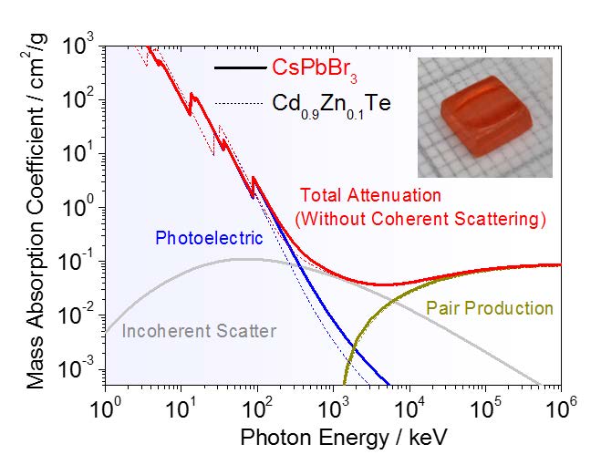
Figure 1. Comparison of the mass absorption coefficient of high energy photons (X- or γ-rays) with energy from 1 keV to 103 MeV in CdZnTe (Cd0.9Zn0.1Te) and CsPbBr3. Note the inset is a polished single CsPbBr3 crystal with size of 5x5x2 mm3 grown by Bridgman method.
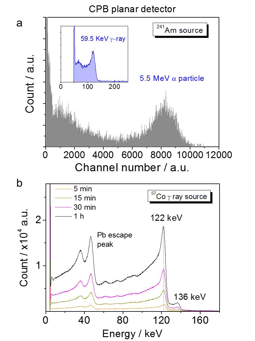
Figure 2. (α) particle and γ-ray spectrum from 241Am isotope resolved by In/CsPb-Br3/Au detector. The applied voltage is -90V for hole collection and shaping time is 2 μs. These two distinct radiations originated from two decay modes, generating both α particle and γ-ray from 241Am. (b) High energy resolution 57Co γ-ray spectra resolved by a Ga/CsPbBr3/Au detector with a shaping time of 2 μs over a continuous collection time of 1 hour.
Detector Performance of CPB Planar Detector
CPB crystallizes in a perovskite structure (Pbnm) and features a bandgap of 2.3 eV, larger than CZT’s 1.65 eV. It melts congruently at 550 degrees Celsius with negligible partial pressure for each component, facilitating melt growth.
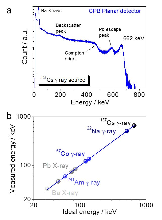
Figure 3. (a) 137Cs γ-ray spectrum resolved by a Ga/CsPbBr3/Au detector with a shaping time of 0.5 μs. The dimension of the detector is 4x2x1.24 mm3. (b) Highly linear detection response of the CsPbBr3 planar detector Ga/CsPbBr3/Au) over a large energy range. Note that each collection was done under the exact same test conditions (-1100 V, 0.5 μs shaping time). The γ-ray sources used were 1 μCi 241Am 59.5 keV and 0.2 mCi 57Co 122 keV and 5 μCi 137Cs 662 keV γ-ray sources, Ba Kα X-ray (32.2 keV) from the 137Cs decays and Pb escape X-ray excited by the 57Co γ-ray.
Centimeter-size, crack-free, large single crystal ingots could be grown with very high purity (below 10 ppm of total impurities) and low defect density using the Bridgman method.
CPB is also air stable, non-hydroscopic, and possesses high effective atomic number Zeff of 65.9, which is much larger than that of CZT (Zeff of 50.2). Thus, the mass absorption coefficient of CPB for high energy photons is higher than CZT in the high energy region (100–500 keV, mainly attributed to the larger cross-section of photoelectric interaction in CPB), as indicated in Figure 1.
Taking 57Co 122 keV γ-ray, for example, the calculated attenuation lengths are 1.70 mm for CZT, and only 1.20 mm for CPB—which is about 30 percent shorter. These features are also superior to typical scintillation materials, such SrI2:Eu and LaBr3:Ce, which are highly hydroscopic and have relatively low effective atomic numbers of Zeff 49.4 and 44.1, respectively.
CPB perovskite’s defect tolerance tends to screen electrically activated defects, which enables the remarkable transport properties of both carriers (> 1×10⁻³ cm2/V for h; > 8×10⁻⁴ cm2 /V for e) [16, 18]. It is useful to have balanced electron and hole transport properties at RT in CPB, since electron transport behaves much better than hole in all other conventional semiconductors.
A device designed with asymmetrical electrode materials (Ga/CsPbBr3/Au or In/ CsPbBr3 /Au) was devised to suppress the leakage current under high electric field, and enable a high level of energy resolving capabilities [16]. Sensing charged particles, such as heavy particles (including α particle) and energetic electrons (β), is particularly important, since they occur as byproducts in numerous radiation decays or nuclear reactions. The In/CsPbBr3/Au detector was fabricated and utilized for detecting α particle from a noncollimated 241Am radiation source.
As indicated in Figure 2a, it clearly resolved both the dominant α particle peak (5.5 MeV) in the high channel number and the accompanying low energy γ-ray peak (59.5 keV). The energy resolution for α particle peak (full width at half maximum, FWHM in percent) was calculated at ~15 percent in Figure 2a. Note that the measured kinetic energy of α particle is somewhat lower than the nominal kinetic energy (5.5 MeV), due to small penetration length and energy loss of α particles through the air (<5 mm) and the In electrode (~70 nm). Fine device design should be optimized to achieve even more accurate measurements.
Device optimization for γ-ray detection for better energy resolution is underway. High energy resolution response from high quality CPB perovskite single crystals has been demonstrated for the first time [16], as depicted in Figure 2b. Specifically, the 57Co γ-ray spectra resolved by a planar CPB detector achieves the energy resolution of 3.9 percent (see Figure 2b), comparable to the commercial CZT detector’s 4.2 percent energy resolution [16]. The CPB detector’s spectroscopic response has been independently verified by researchers at the University of Michigan and Fisk University. Detector performance is also temporally stable (see Figure 2b), implying the potential absence of the charge-trapping induced polarization [16].
Besides 57Co γ-ray, such a planar CPB detector could resolve the 59.5 keV (241Am γ-ray), 511 keV (22Na γ-ray) and 662 keV (137Cs γ-ray) peaks as well, while the representative 137Cs γ-ray spectrum was demonstrated in Figure 3a. The energy resolution (FWHM in percent) for 137Cs 662 keV γ-ray peak is about 3.8 percent. For semiconductor radiation detectors, the spectroscopic linearity is usually very good, with intrinsically absent nonproportionality response [19]. Our results, shown in Figure 3b, also confirm the semiconductor CPB detector’s excellent linearity response, as would be expected from a semiconductor. This characteristic is superior to scintillation materials [20], such as NaI:Tl and LaBr3 :Ce, which suffer from the change of light yield at low energies.
In consideration of these favorable properties (low cost, readily scale-up, robust high performance), it is reasonable to propose CPB as an exceptionally viable material for next-generation radiation detectors for use at room temperature.
Potential Applications
One of the most important types of radiation emitted from fissile materials is γ-rays of a wide variety of energies. CPB detectors could be used for detecting X- and γrays in a wide energy range (see Figure 1), offering excellent energy resolution in an affordable form factor. Thus, CPB detectors could be deployed widely in homeland security applications, such as identifying dirty bombs, radioactive bombs, and radiological dispersion devices, or in seeking an unidentified radiological source, as can happen in any circumstance that involves a fissile material (such as 235U, used in nuclear power electricity generation).
In addition, based on CPB detectors, handheld or portable radiological identification devices could be developed, on account of CPB’s strong stopping power. Due to its low cost and high energy resolution for gamma ray radiation, CPB could meet rising market demands, and meet the health and safety standards for low-dose radiation (due to its relatively low mobility 15). In the U.S., 90 percent of all non-homeland defense and security-related uses of X- and γ- ray devices are in medical imaging, and CPB detectors might also be considered for novel medical applications.
Discussion
In summary, perovskite material CPB has demonstrated the exceptional potential for next-generation detection of X- and γray radiation as well as charged particles. CPB’s unique crystal structure and dynamic lattice lead to strong defect tolerance and unprecedented long carrier lifetime, which is unusual compared to conventional semiconductors CZT and TlBr. Due to their excellent charge transport properties and uniformity, the CPB detectors have showed comparable performance with state-of-art CZT detectors. CPB can be produced at lower costs than CZT or TlBr due to the readily accessibility of CsBr and PbBr2 binaries.
Device fabrication processes such as electrode screening and optimization should be explored further to unlock the full potential of detection performance. For applications to detect high energy γ-rays, a high performance single crystal of CPB with large volume (over 1 cm3) should be a top R&D priority. Further efforts should also focus on crystal growth engineering and device fabrication. Integration of CPB detectors into current or new digital detection systems (such as the compton camera) is also desirable. Additional fundamental research into perovskites may enable further advances in radiation detection. Though inclusions or precipitates are absent in CPB single crystal, other micro-structural defects which play an important role in degrading the detector performance should also be investigated or eliminated further.
References
1. Wahl, C. G., Kaye, W. R., Wang, W., Zhang, F., Jaworski, J. M., King, A., . . . & He, Z. (2015). The Polaris-H imaging spectrometer. Nuclear Instruments and Methods in Physics Research Section A: Accelerators, Spectrometers, Detectors and Associated Equipment, 784, 377–381. doi:10.1016/j. nima.2014.12.110
2. Veale, M. C., Bell, S. J., Jones, L. L., Seller, P., Wilson, M. D., Allwork, C., . . . & Cernik, R. C. (2011). An ASIC for the study of charge sharing effects in small pixel CdZnTe X-Ray detectors. IEEE Transactions on Nuclear Science, 58(5), 2357–2362. doi:10.1109/tns.2011.2162746
3. Gehrels, N., Chincarini, G., Giommi, P., Mason, K. O., Nousek, J. A., Wells, A. A. . . . & Roming, P. W. A. (2004). The swift gamma-ray burst mission. AIP Conference Proceedings, 727, 637–641. doi:10.1063/1.1810924
4. Novikov, V. (2018, April 16). The M2PRDS represents an alternative acquisition approach. Retrieved from https://www.army.mil/article/203934/the_m2prds_represents_an_alternative_acquisition_approach
5. Loef, E. V., Wilson, C. M., Cherepy, N. J., Hull, G., Payne, S. A., Choong, W., . . . & Shah, K. S. (2009). Crystal growth and scintillation properties of strontium iodide scintillators. IEEE Transactions on Nuclear Science, 56(3), 869–872. doi:10.1109/tns.2009.2013947
6. Alekhin, M. S., Haas, J. T., Khodyuk, I. V., Krämer, K. W., Menge, P. R., Ouspenski, V., & Dorenbos, P. (2013). Improvement of γ-ray energy resolution of LaBr3 :Ce3+ scintillation detectors by Sr2+ and Ca2+ co-doping. Applied Physics Letters, 102(16), 161915. doi:10.1063/1.4803440
7. Zhang, F., Herman, C., He, Z., Geronimo, G. D., Vernon, E., & Fried, J. (2012). Characterization of the H3D ASIC readout system and 6.0 cm3 3-D position sensitive CdZnTe detectors. IEEE Transactions on Nuclear Science, 59(1), 236–242. doi:10.1109/tns.2011.2175948
8. Hofstadter, R. (1947). Thallium halide crystal counter. Physical Review, 72(11), 1120– 1121. doi:10.1103/physrev.72.1120
9. He, Z., Knoll, G., Wehe, D., & Miyamoto, J. (1996, November 2–9). Position sensitive single carrier CdZnTe detectors. 1996 IEEE Nuclear Science Symposium. Conference Record. doi:10.1109/nssmic.1996.590973
10. He, Z., Li, W., Knoll, G., Wehe, D., Berry, J., & Stahle, C. (1999). 3-D position sensitive CdZnTe gamma-ray spectrometers. Nuclear Instruments and Methods in Physics Research Section A: Accelerators, Spectrometers, Detectors and Associated Equipment, 422(1–3), 173-178. doi:10.1016/s0168-9002(98)00950-4
11. Szajnfarber, Z. (2011, June). Innovation Pathways in Technology Intensive Government Organizations: Insights from NASA (Doctoral Dissertation). Massachusetts Institute of Technology, Cambridge, MA. Retrieved from https://dspace.mit.edu/handle/1721.1/67758
12. Johnsen, S., Liu, Z., Peters, J. A., Song, J., Nguyen, S., Malliakas, C. D., . . . & Kanatzidis, M. G. (2011). Thallium chalcohalides for X-ray and γ-ray detection. Journal of the American Chemical Society, 133(26), 10030–10033. doi:10.1021/ja202540t
13. Lin, W., Stoumpos, C. C., Liu, Z., Das, S., Kontsevoi, O. Y., He, Y., . . . & Kanatzidis, M. G. (2017). TlSn2I5, a robust halide antiperovskite semiconductor for γ-Ray detection at room temperature. ACS Photonics, 4(7), 1805–1813. doi:10.1021/acsphotonics.7b00388
14. He, Y., Kontsevoi, O. Y., Stoumpos, C. C., Trimarchi, G. G., Islam, S. M., Liu, Z., . . . & Kanatzidis, M. G. (2017). Defect antiperovskite compounds Hg3Q2I2 (Q = S, Se, and Te) for room-temperature hard radiation detection. Journal of the American Chemical Society, 139(23), 7939–7951. doi:10.1021/jacs.7b03174
15. Wang, P. L., Liu, Z., Chen, P., Peters, J. A., Tan, G., Im, J., . . . & Kanatzidis, M. G. (2015). Hard radiation detection from the selenophosphate Pb2P2Se6. Advanced Functional Materials, 25(30), 4874–4881. doi:10.1002/adfm.201501826
16. He, Y., Matei, L., Jung, H. J., Mccall, K. M., Chen, M., Stoumpos, C. C., . .. & Kanatzidis, M. G. (2018). High spectral resolution of gamma-rays at room temperature by perovskite CsPbBr3 single crystals. Nature Communications, 9(1). doi:10.1038/s41467- 018-04073-3
17. Stoumpos, C. C., Malliakas, C. D., Peters, J. A., Liu, Z., Sebastian, M., Im, J., . . . & Kanatzidis, M. G. (2013). Crystal growth of the perovskite semiconductor CsPbBr3: A new material for high-energy radiation detection. Crystal Growth & Design, 13(7), 2722–2727. doi:10.1021/cg400645t
18. He, Y., Liu, Z., McCall, K. M., Lin, W., Chung, D. Y., Wessels, B. W., & Kanatzidis, M. G. (2019, April). Perovskite CsPbBr3 single crystal detector for alpha-particle spectroscopy. Nuclear Instruments and Methods in Physics Research, 922, 217–221.
19. Owens, A., Buslaps, T., Gostilo, V., Graafsma, H., Hijmering, R., Kozorezov, A., . . . & Welter, E. (2006). Hard X- and γ-ray measurements with a large volume coplanar grid CdZnTe detector. Nuclear Instruments and Methods in Physics Research Section A: Accelerators, Spectrometers, Detectors and Associated Equipment, 563(1), 242–248. doi:10.1016/j.nima.2006.01.120
20. Lecoq, P. (2016). Development of new scintillators for medical applications. Nuclear Instruments and Methods in Physics Research Section A: Accelerators, Spectrometers, Detectors and Associated Equipment, 809, 130–139. doi:10.1016/j.nima.2015.08.041